Our Services 业务体系
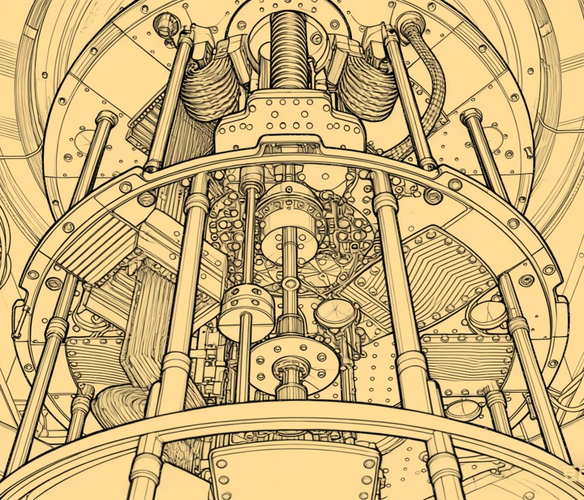
Custom Quantum Chip Fabrication 量子芯片代工
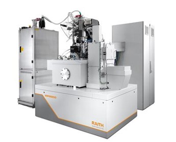
Advanced superconducting qubit nanofabrication: Full-stack services from tape-out to wafer-level manufacturing.
[ E-Beam Lithography (100kV) ]
[Resolution] Min linewidth ≤8nm@100μm
[Accuracy] Stitching ≤15nm, Overlay ≤5nm
[Capacity] Pieces to 8" wafers, 1000μm field
[ Dual-Angle E-Beam Evaporation ]
[Temp/Uniform] ≥1000℃ / ≤2%
[Oxidation] ±75° tilt, static & dynamic control
[ Precision Dicing & Flip-chip Bonding ]
先进超导量子比特纳米制造:从流片到晶圆级制造的全栈服务。
【电子束曝光设备 100kV】
【分辨率】最小线宽≤8nm @100μm
【精度】拼接≤15nm, 套刻≤5nm
【尺寸】兼容散片至8英寸晶圆, 写场1000μm
【双倾角电子束蒸发系统】
【温控/均一】最高≥1000℃ / ≤2%
【离子铣/氧化】倾角±75°, 静态与动态可控
【精准切割与倒装贴片】
Single-chip 10-qubit 单芯片10比特
[Shipping] Standard Product
[Topology] 1D Chain
[Qubits] Tunable / Fixed Coupling
[Freq] Readout 6.7-7.5GHz, Qubit 5.3-5.6GHz
[T1 / T2*] Avg. 35μs / Avg. 30μs
[Fidelity] Readout 95%, 1Q >99.8%, CZ >98%
[Applications] Non-equilibrium dynamics, lattice gauge fields, GHZ states.
[Custom] Variable counts & params, tunable couplers.
【出货状态】公版出货
【构型】一维链状
【比特/耦合】频率可调 / 固定耦合
【频率】读取腔 6.7-7.5GHz, Qubit 5.3-5.6GHz
【T1 / T2*】平均35μs / 平均30μs
【保真度】读取95%, 单比特>99.8%, CZ>98%
【适用场景】非平衡动力学研究、晶格规范场模拟、多比特GHZ态。
【定制改版】比特数与参数可调,支持增加可调耦合器。
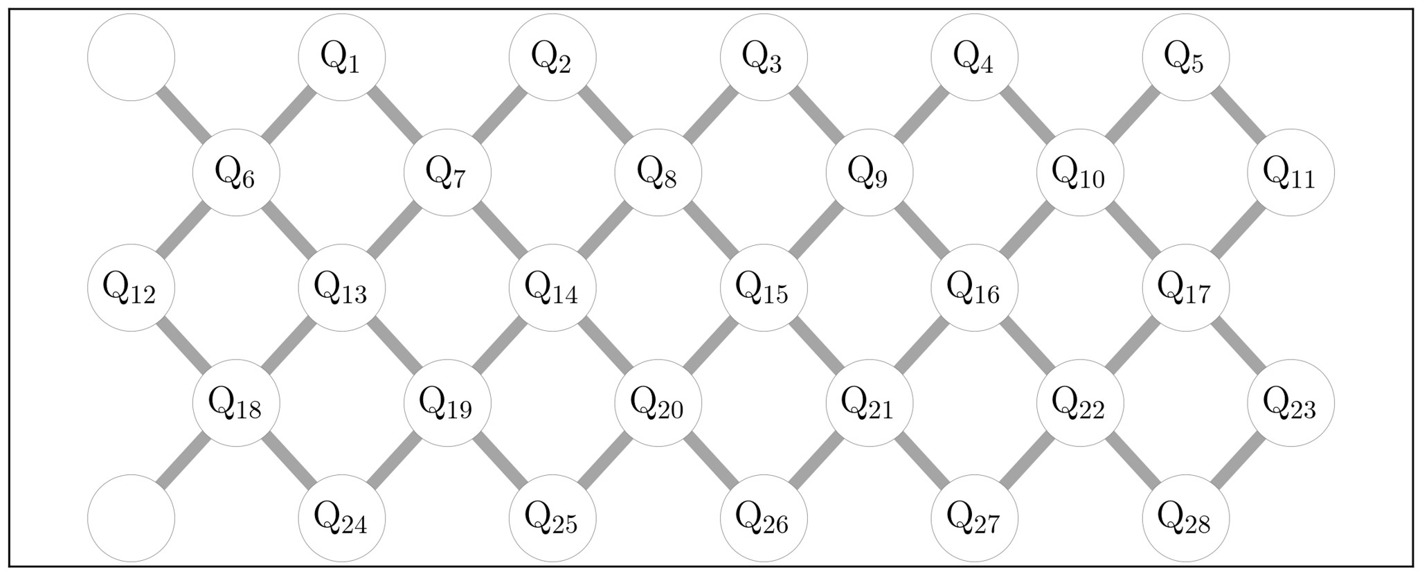
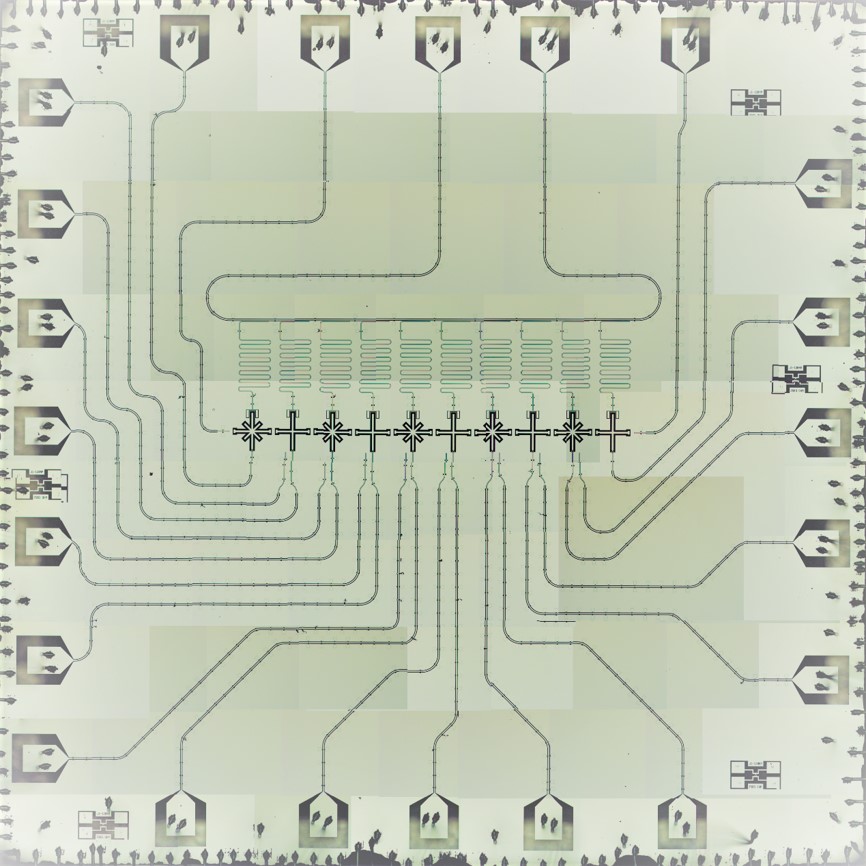
28-qubit Flip-Chip 28比特倒装芯片
[Shipping] Standard Product
[Topology] 2D Square Lattice (Flip-chip)
[Qubits] Tunable / Tunable Coupling
[Freq] Readout 6.7-7.2GHz, Qubit 5-5.3GHz
[T1 / T2*] Avg. 50μs / Avg. 30μs
[Fidelity] Readout 95%, 1Q >99.9%, CZ >99%
[Features] Purcell filter, XY & Z crosstalk < 1%
[Applications] Surface code experiments, various quantum simulations.
[Custom] Variable counts & params, optional reset components.
【出货状态】公版出货
【构型/封装】2D Square Lattice / 倒装
【比特/耦合】频率可调 / 耦合可调
【频率】读取腔 6.7-7.2GHz, Qubit 5-5.3GHz
【T1 / T2*】平均50μs / 平均30μs
【保真度】读取95%, 单比特>99.9%, CZ>99%
【附加组件】Purcell filter, XY及Z信号串扰<1%
【适用场景】表面码实验、各种量子模拟实验。
【定制改版】比特数与参数可调,可加入reset组件。
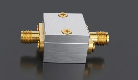
Josephson Parametric Amplifier 约瑟夫森参量放大器
[Shipping] Standard Product
[Packaging] Chip packaged within a dual-port sample box
[Frequency] 6-8 GHz
[Gain/Bandwidth] Bandwidth ≥ 400MHz @ Gain ≥ 15dB
[Noise Temp] < 400 mK
[Applications] Multi-qubit readout, small signal measurement, dark matter detection, etc.
【出货状态】公版出货
【封装】芯片已封装于双端口样品盒内
【工作频率】6-8 GHz
【增益与带宽】大于15dB的增益带宽大于400 MHz
【噪声温度】低于400 mK
【适用场景】多量子比特读出、小信号测量和暗物质探测等。
Test & Analysis 测试分析服务
Providing wafer-level mK ultra-low temperature automated testing and advanced characterization analysis.
[ Basic Services ]
• Cryogenic wiring installation
• Custom brackets & sample enclosures
• RT control system setup & noise mitigation
• Software & data pipeline deployment
• Basic chip parameter calibration
[ Advanced Services ]
• Pre-calibration (crosstalk, distortion, timing)
• High-fidelity 1Q/2Q gate calibration & benchmark
• Advanced techniques for quantum simulation
提供晶圆级mK级极低温自动化测试以及高级特性分析服务。
【基本服务】
• 低温测试线路的安装
• 挂架与样品盒的定制化设计
• 室温测控系统的搭建与环境噪声排查
• 测控软件及基本数据处理程序的部署与调试
• 芯片基本参数的标定
【高级服务】
• 串绕、信号失真、时序对齐等前期校正方法
• 高保真度单双量子门的校准与benchmark方法
• 与量子模拟相关的高阶实验技巧